Precision Etching Beryllium Copper
Previous
Next
Wonder Copper(BE-CU.COM) has a reputation for precision etching quality parts from Beryllium Copper.Capable of handling parts sizes from 0.02 in. dia. to 24 x 60 in. and 0.001 to 0.08 in. thickness.
Introducing Wonder's "beryllium copper parts and products". Wonder copper will continue to develop and machining beryllium copper that support the foundation of society and help solve environmental issues.
Beryllium copper Etching products
- Electronics
- Microelectronics
- Aerospace
- Tooling and Molds
- Medical Devices
- Telecommunications
- Precision Instruments
- More
Beryllium copper is commonly used in electronic components due to its excellent electrical conductivity and spring properties. Etching can be used to create intricate patterns or fine-tune the shapes of electrical contacts, connectors, and other components.In the microelectronics industry, beryllium copper is often used in microelectromechanical systems (MEMS) and integrated circuits. Etching allows for precise shaping of beryllium copper structures at the micron level, enabling the fabrication of miniaturized components and devices.Etching can be used to fabricate lightweight yet durable components such as heat sinks, springs, and connectors for aerospace systems.Beryllium Copper Etching enables the production of intricate components for devices such as surgical instruments, pacemakers, and implantable sensors.
Beryllium copper's combination of electrical conductivity and mechanical strength makes it suitable for telecommunications applications. Etching can be utilized to fabricate high-performance components like connectors, antennas, and transmission lines for telecommunications infrastructure.Beryllium copper is used in precision instruments where dimensional stability and reliability are critical. Etching allows for the fabrication of precise components such as springs, contacts, and sensor elements in devices like measuring instruments and scientific equipment.
Beryllium Copper Etching Services
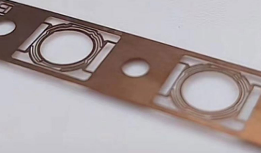
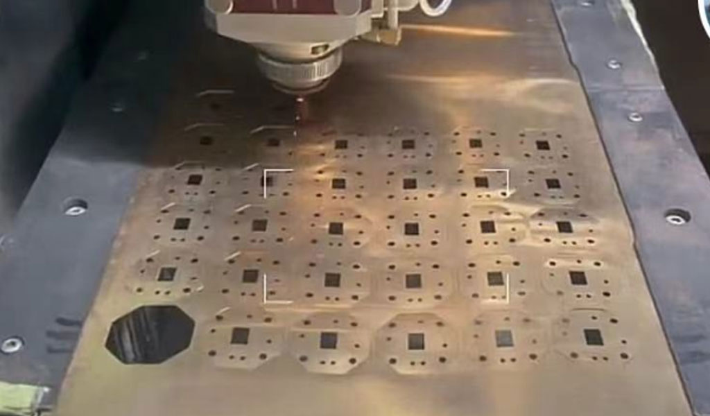
The conventional method for etching beryllium copper plates typically involves either stamping or laser processing. However, stamping processes struggle with burrs and oil contamination issues, and maintaining processing precision can be challenging. BE-CU employs chemical etching, resulting in high precision, burr-free products, with flexible design alteration capabilities.
To effectively manufacture such precision products, the primary requirement is the availability of a purified production workshop. The size, width, presence of breakpoints, and recesses in the mesh of etched beryllium copper plates will undoubtedly affect product correctness and filtration sensitivity in the future. Our purification workshop operates at a level of cleanliness reaching ten thousand, a prerequisite for processing such products! Additionally, we possess multiple imported beryllium copper etching production lines to ensure the accuracy of etching processing, along with a comprehensive quality control system to prevent defective products from reaching customers
Collaborating with several Fortune 500 companies, BE-CU provides a compelling reason to choose us! The materials used by the company are primarily imported, enabling etching processing of various materials and making us the preferred domestic alternative to Taiwanese and Japanese production. Depending on material thickness, the minimum aperture can reach 0.05mm, flatness can be maintained below 0.02mm, and the minimum tolerance can achieve +/-0.0075mm.
Excellent Properties Of Beryllium Copper Alloy
High Flexibility
High Hardness
High Strength
High Conductivity
High Thermal Conductivity
Good Molding Properties
Good Fatigue Performance
Excellent Corrosion Resistance
No Spark Impact
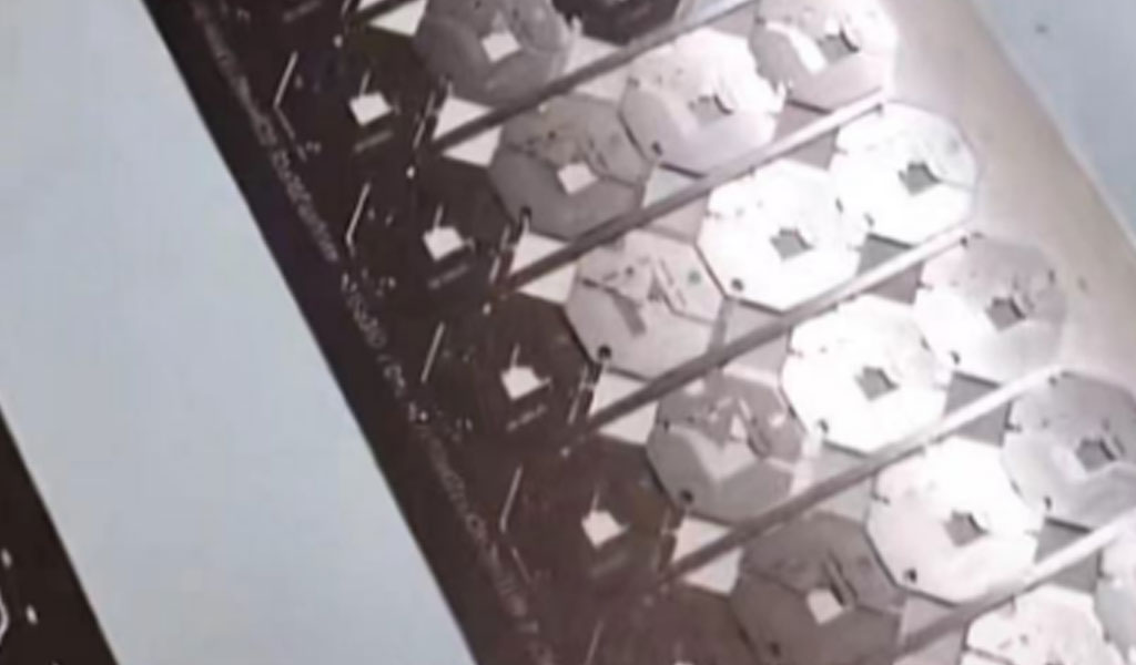
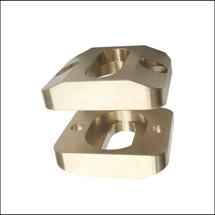
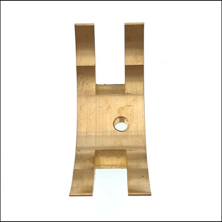
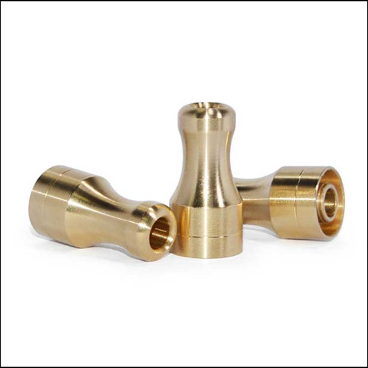
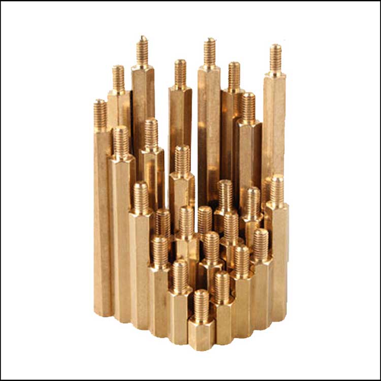
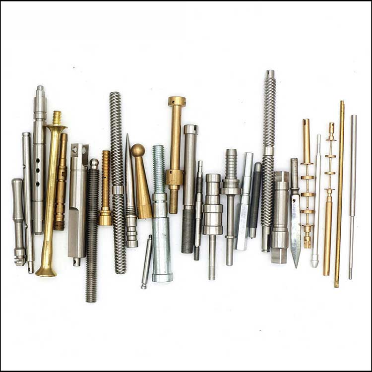
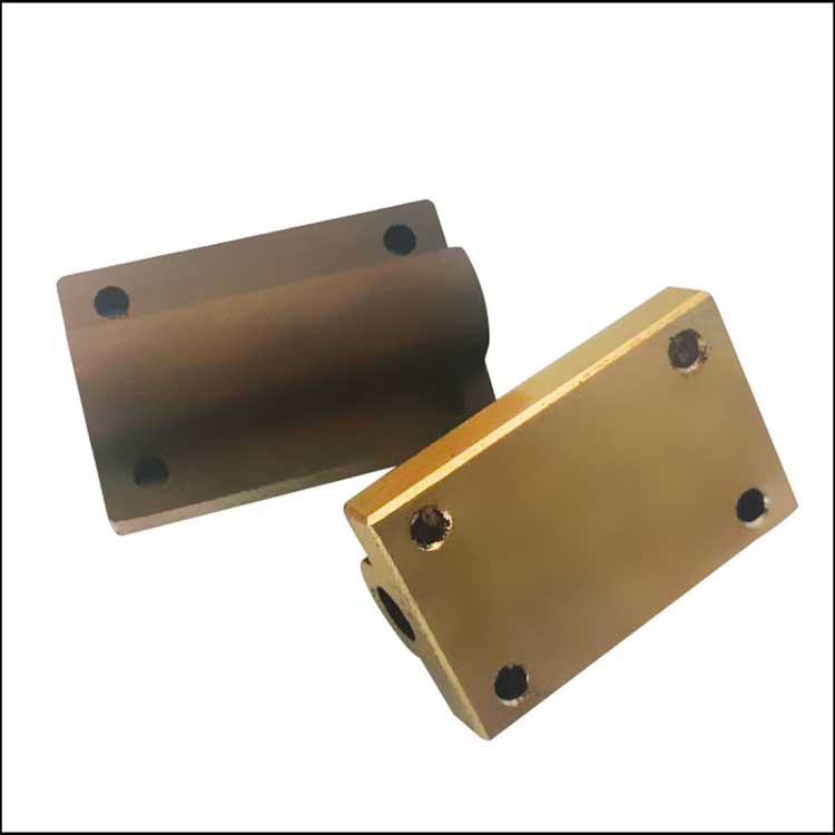
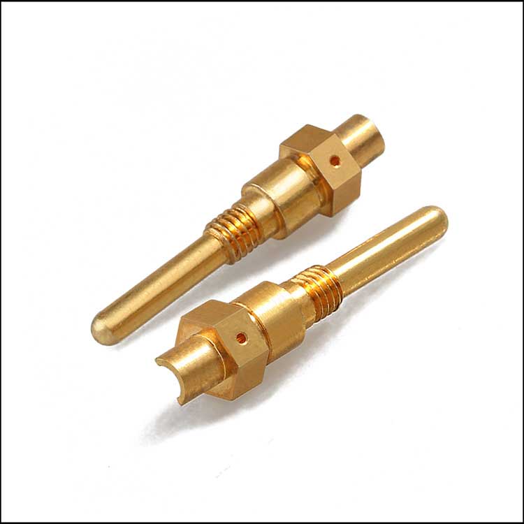
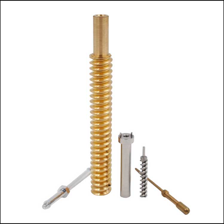
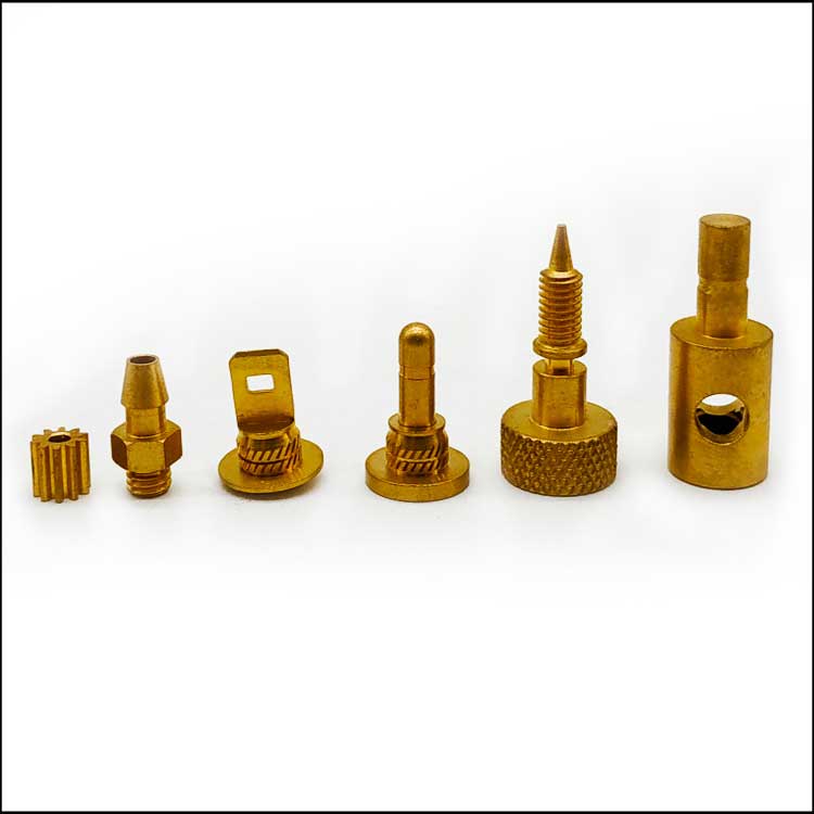
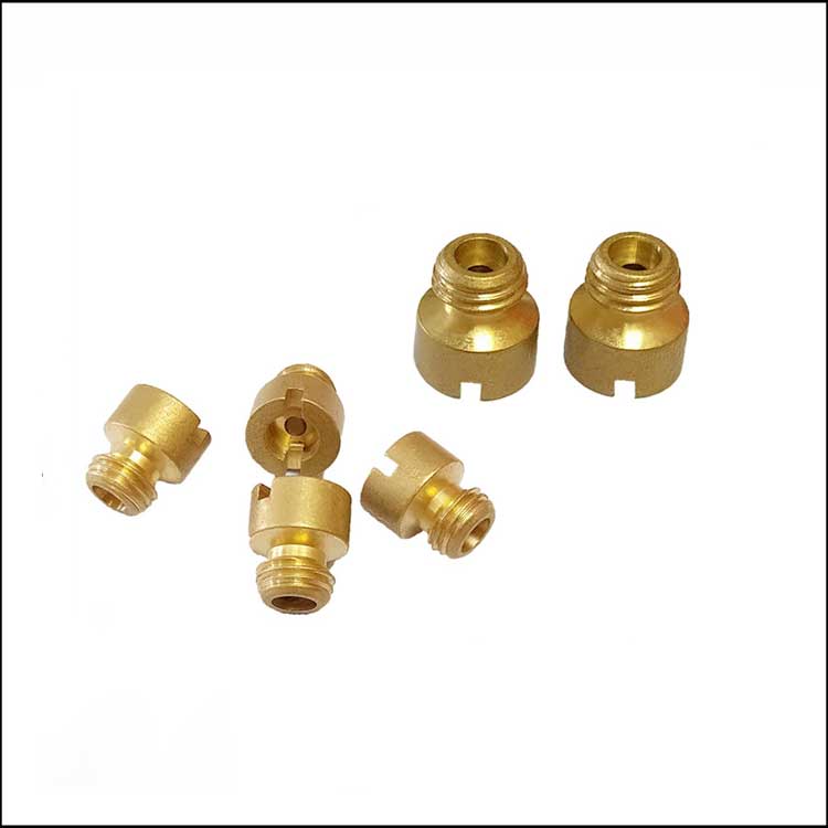
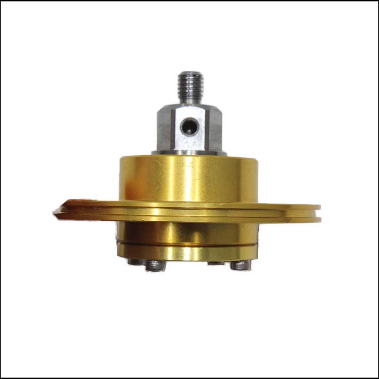
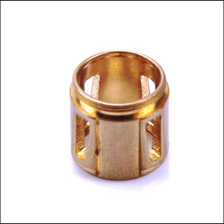
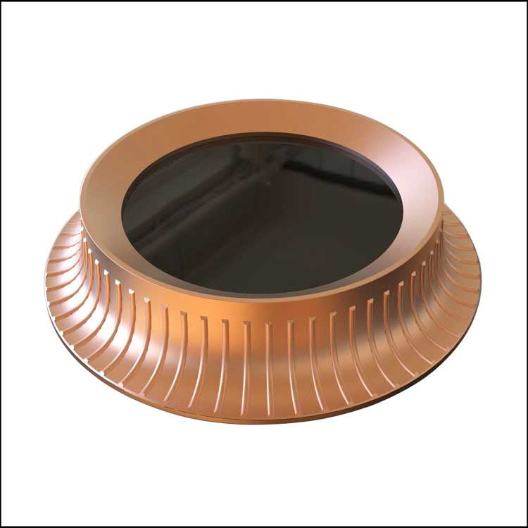
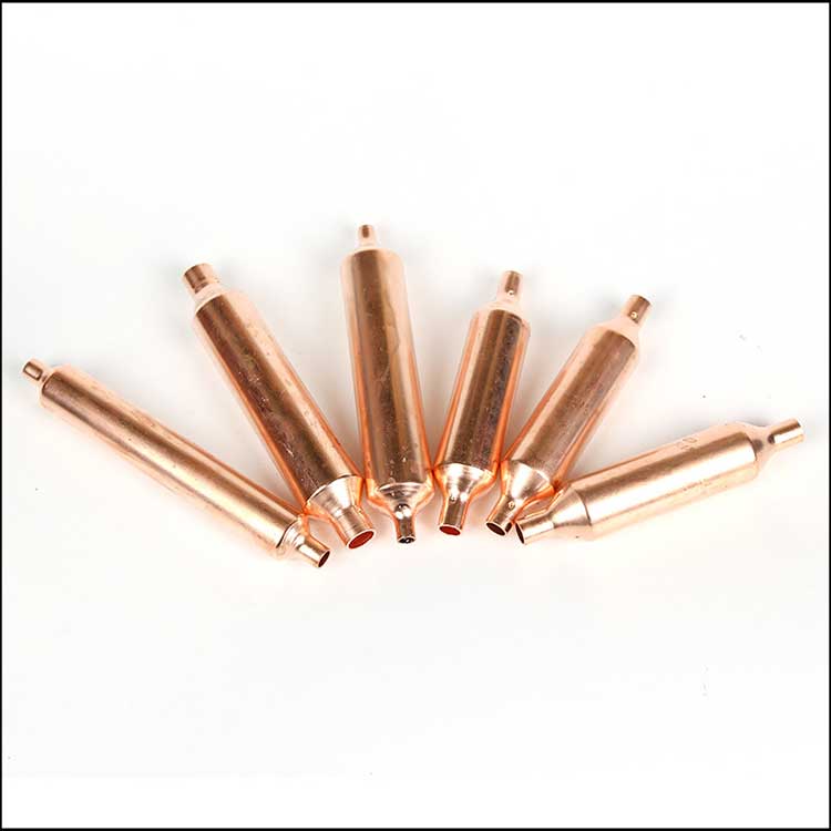
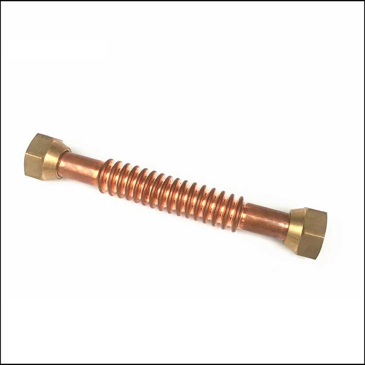
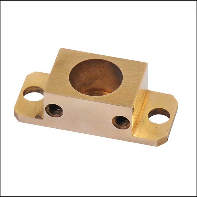
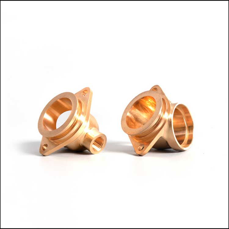
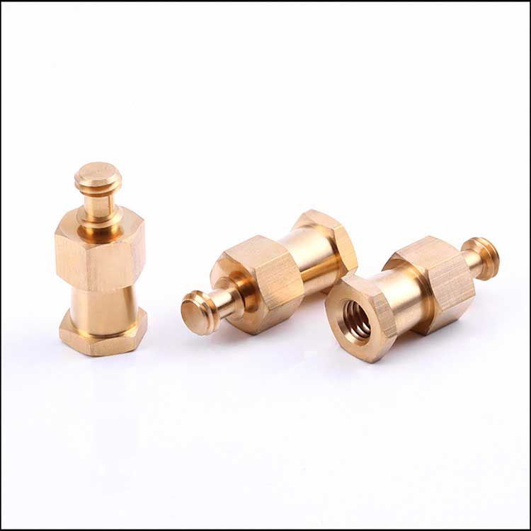
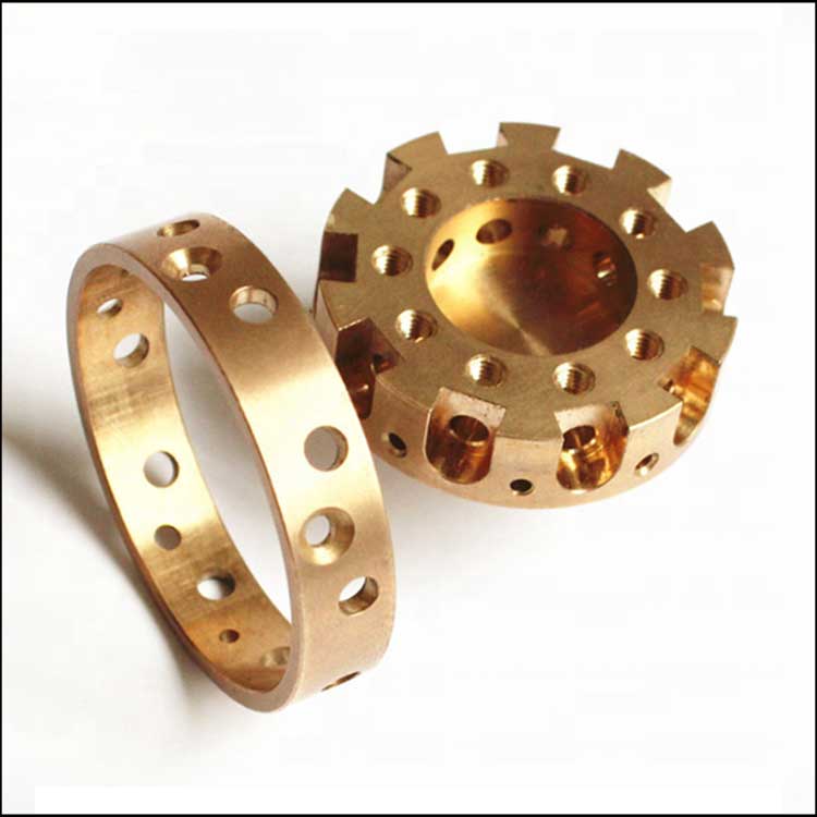
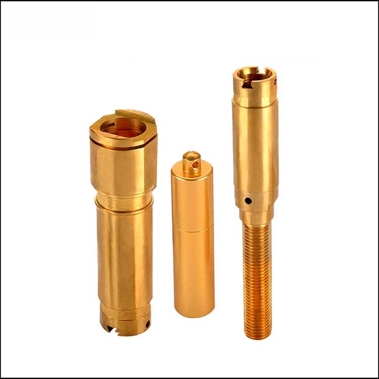
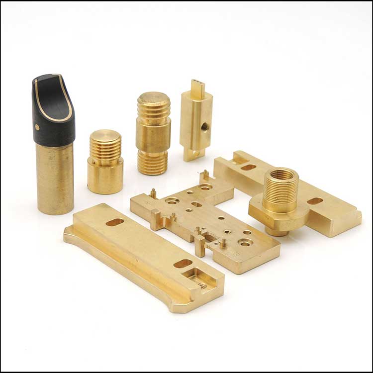
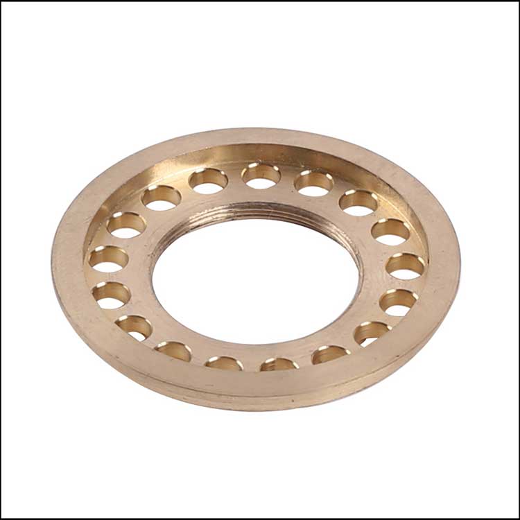
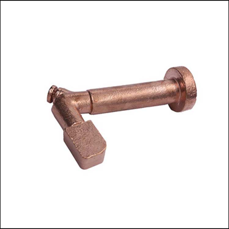
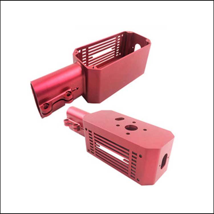
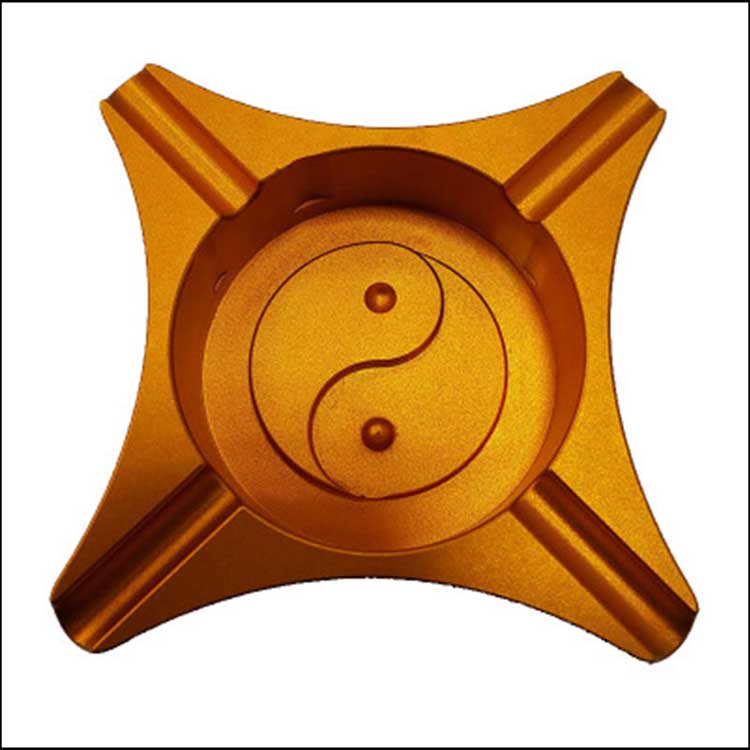
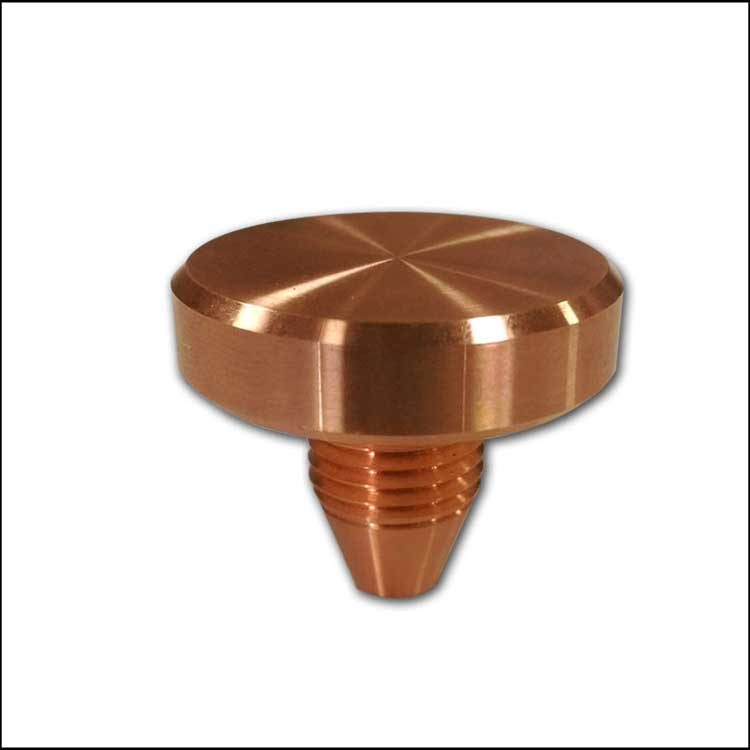
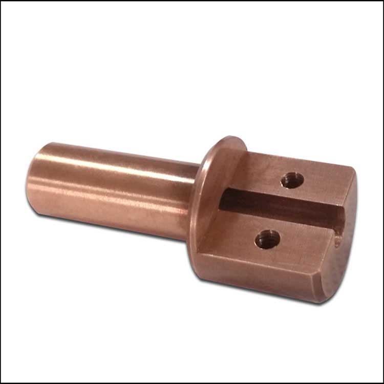
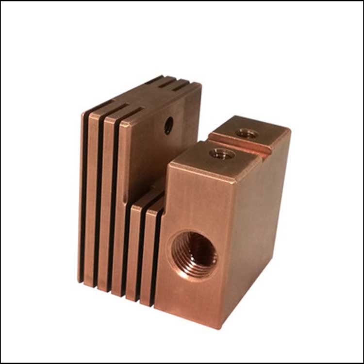
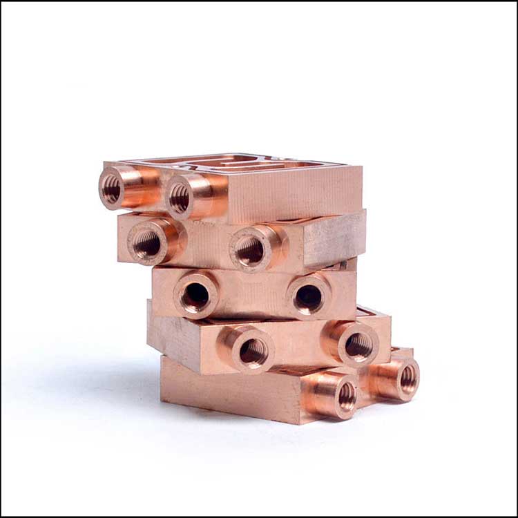
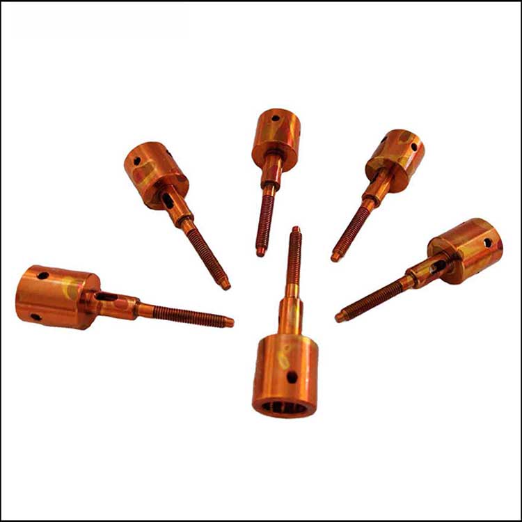
Beryllium Copper Etching Parts Case Studies
-
- beryllium copper parts (3)
-
- beryllium copper parts (4)
-
- beryllium copper parts (5)
-
- beryllium copper parts (6)
-
- beryllium copper parts (7)
-
- beryllium copper parts (8)
-
- beryllium copper parts (9)
-
- beryllium copper parts (10)
-
- beryllium copper parts (11)
-
- beryllium copper parts (12)
-
- beryllium copper parts (13)
-
- beryllium copper parts (14)
-
- beryllium copper parts (15)
-
- beryllium copper parts (16)
-
- beryllium copper parts (17)
-
- beryllium copper parts (18)
-
- beryllium copper parts (19)
-
- beryllium copper parts (20)
-
- beryllium copper parts (21)
-
- beryllium copper parts (22)
-
- beryllium copper parts (23)
-
- beryllium copper parts (24)
-
- beryllium copper parts (25)
-
- beryllium copper parts (26)
-
- beryllium copper parts (27)
-
- beryllium copper parts (28)
-
- beryllium copper parts (29)
-
- beryllium copper parts (30)
-
- beryllium copper parts (1)
-
- beryllium copper parts (2)
Chemical Composition
Executive standard:ASTM/GB/T5233-2001/EN12163(%max., unless shown as range or min.)
Numbering
Be
Co+Ni
Cu
Fe
Pb
Si
Al
C17200
1.8-2.0
Co+Ni≥0.2
Margin
0.15
-
0.15
0.15
C17300
1.8-2.0
Co+Ni≥0.2
Margin
0.15
0.2-0.6
0.15
0.15
C17500
0.4-0.7
Co 2.4-2.7
Margin
0.15
-
0.15
0.15
C17510
0.2-0.6
Co≤0.3,Ni 1.4-2.2
Margin
0.15
-
0.15
0.15
QBe2.0
1.8-2.1
Ni 0.2-0.5
Margin
0.15
0.005
0.15
0.15
BeCo1Ni1
0.4-0.7
Co 0.8-1.3,Ni 0.8-1.3
Margin
0.02
-
0.02
0.04
Mechanical properties and conductivity analysis
(AT/TF00)
Numbering
Tensile Strength /MPa
Yield Strength /MPa
Elongation %
Hardness
Conductivity %IACS
C17200
1160-1380
980-1240
3—15
36-42HRC
22-28
C17300
1160-1380
980-1240
3—15
36-42HRC
22-28
C17500
700-920
560-710
10—25
92-100HRB
45-60
C17510
700-920
560-710
10—25
92-100HRB
45-60
QBe2.0
1160-1380
980-1240
3—15
36-42HRC
18-20
BeCo1Ni1
700-920
560-710
10—25
92-100HRB
45-60
Available status
Brush Name
ASTM Name
Description
A
TB00
Solution annealing state (quenched state)
¼H
TD01
Quarter hard
½H
TD02
Half hard (semi-hard)
¾H
TD03
Three-quarters hard
H
TD04
Hard state (full hard)
AT
TF00
Standard aging heat treatment in quenched state
¼HT
TH01
Quarter hard standard aging heat treatment
½HT
TH02
Half-hard standard aging heat treatment
¾HT
TH03
Three-quarters hard standard aging heat treatment
HT
TH04
Hard standard aging heat treatment (a process of comprehensive strengthening of deformation and aging)
Note: In the Brush name:
- "A" represents the state of solution annealing (annealed, the alloy is in the softest state, easy to be stamped and formed, and needs to be cold worked or strengthened during the direct failure period);
- "H" stands for cold processing state (hard);
- "T" means that the material has been aging hardened by standard heat treatment (heat treatment means the state of aging strengthening heat treatment).